Contents
- 1 Introduction
- 2 Understanding Chiplet Architecture in CPU Design
- 3 How Chiplet Design Enhances Scalability
- 4 Cost Benefits of Modular Processor Design
- 5 Manufacturing Flexibility and Advanced Packaging Techniques
- 6 Challenges and Considerations for Chiplet CPUs
- 7 Conclusion
- 8 Frequently Asked Questions (FAQ)
Introduction
The world of CPU design is undergoing a transformative shift. Traditional monolithic CPU architectures where a processor is created as a single, large silicon die are increasingly challenged by physical, economic, and engineering limits. Enter chiplet architecture, a modular approach that assembles multiple smaller chips or ‘chiplets’ into a unified processor. This approach is quickly gaining momentum among leading semiconductor makers. But why are future CPUs moving away from one-piece designs? In this article, we’ll delve into the evolution of chiplet design, exploring how it improves scalability, drives down costs, and enhances manufacturing flexibility in CPU architecture.
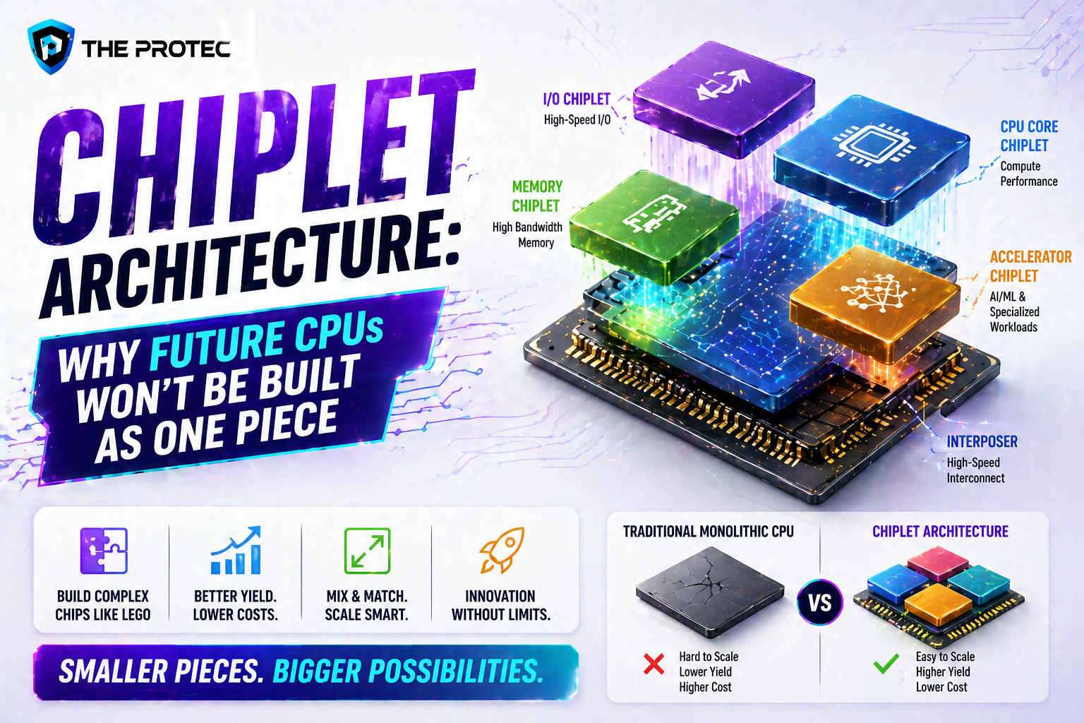
Understanding Chiplet Architecture in CPU Design
Traditional CPUs are crafted as monolithic dies, which means all elements cores, cache, I/O controllers reside on a single silicon wafer. While this design evolved with leaps in semiconductor lithography, it now faces significant challenges:
- Yield Limitations: Larger dies are more susceptible to defects, drastically lowering production yields.
- Escalating Costs: Increased wafer sizes and lower yields hike up fabrication expenses.
- Thermal and Power Constraints: Packing everything into one die intensifies heat dissipation and power distribution complexities.
- Design Complexity: Integrating heterogeneous components complicates design and innovation timelines.
Chiplet architecture offers a solution by breaking down the CPU into multiple smaller dies that can be manufactured separately and then integrated into a multi-chip module (MCM). Each chiplet specializes in specific functions such as one for CPU cores, another for cache, and others for I/O or accelerators interconnected via advanced high-speed interfaces.
How Chiplet Design Enhances Scalability
One of the chief advantages of chiplet-based modular processors is improved scalability. Instead of designing and manufacturing increasingly complex monolithic dies, engineers can scale performance by adding more chiplets or specialized dies in a flexible manner. Here’s how chiplet design boosts scalability:
1. Incremental Performance Growth
Chiplets allow semiconductor companies to add processing cores or cache blocks via additional dies without redesigning an entirely new monolithic chip. This modular methodology accelerates the pace of innovation, enabling rapid introduction of higher core counts and new capabilities without a full chip redesign.
2. Heterogeneous Integration
With chiplet architecture, different process technologies can coexist neatly. For example, CPU core chiplets may leverage cutting-edge 3nm nodes optimized for high performance, while cache or I/O chiplets might utilize more mature and cost-effective nodes. This adaptability makes it easier to balance performance with power and cost considerations while expanding CPU capabilities.
3. Easier Customization and Variability
Chiplet designs also facilitate tailored CPU configurations for diverse market segments. Data center processors can incorporate dozens of core chiplets for maximum throughput, while consumer CPUs can be customized with fewer cores but higher frequency chiplets. This flexibility fosters better product differentiation and options at scale.
Cost Benefits of Modular Processor Design
The economics behind chiplet-based CPUs are as compelling as the technical advantages. Manufacturing costs have long been a bottleneck hampering Moore’s Law scaling. Chiplets address this challenge from multiple angles:
1. Improved Manufacturing Yields
Smaller dies are less prone to defects during fabrication. By splitting a large CPU into many chiplets, manufacturers improve overall yield rates. While some chiplets might fail quality control, others can still be assembled into a usable processor, reducing the number of completely wasted chips.
2. Reusability of Chiplets
Chiplets designed for one processor can sometimes be repurposed or slightly modified for others, significantly lowering redesign and validation expenses. This reusability supports faster time-to-market and enables scaling production volumes across different CPU families.
3. Segmented Supply Chain
Because chiplets can be manufactured at different fabs specialized by technology node or geographic location, companies can optimize supply chains for cost and risk mitigation. For example, the high-performance logic chiplets might be produced in a state-of-the-art fab, while analog or I/O chiplets are manufactured in less expensive facilities.
Manufacturing Flexibility and Advanced Packaging Techniques
Chiplet CPU architecture leverages advanced semiconductor packaging technologies that were not fully mature a few years ago. These innovations enable seamless communication among physically separate chiplets, maintaining performance and reliability.
1. 2.5D and 3D Packaging
Techniques such as 2.5D interposers and 3D stacking use silicon or organic substrates to connect chiplets with ultra-high-density wiring. These packaging solutions allow for high bandwidth, low latency, and energy-efficient interconnects vital to matching or even exceeding monolithic CPU performance.
2. Advanced Interconnects and Standards
High-speed interconnects like AMD’s Infinity Fabric or Intel’s Embedded Multi-die Interconnect Bridge (EMIB) facilitate the communication needed for chiplet cohesion. Industry efforts toward standards such as the Open Domain-Specific Architecture (ODSA) work to create interoperability across different chiplet providers and designs.
3. Design Modularity and IP Protection
Separating CPU components into chiplets also allows for enhanced intellectual property (IP) protection. Companies can outsource some chiplets with less critical IP while keeping core designs proprietary. This modular approach boosts collaboration and ecosystem development while preserving competitive advantages.
Challenges and Considerations for Chiplet CPUs
Despite the many advantages, chiplet architecture also introduces challenges that the industry continues to address:
- Inter-chiplet Latency and Bandwidth: Ensuring that communication among chiplets matches on-die speeds demands advanced interconnect tech to minimize performance penalties.
- Power and Thermal Management: Multi-chip modules create complex power delivery and heat dissipation scenarios that require sophisticated engineering solutions.
- Testing and Validation: Assembling chiplets from different sources necessitates extensive validation to ensure reliability and compatibility.
Despite these obstacles, the benefits of chiplet designs have driven semiconductor leaders to invest heavily in overcoming these issues, making chiplet CPUs increasingly prevalent in high-performance computing sectors.
Conclusion
The chiplet design revolution is reshaping the future of CPU architecture. Moving away from monolithic dies toward sophisticated, modular processors unlocks unprecedented scalability, economical manufacturing, and design flexibility. As advanced packaging and interconnect technologies mature, we can expect more powerful, efficient, and customized processors built from chiplets to dominate the market from data centers to consumer electronics.
This architectural paradigm shift equips the semiconductor industry to continue pushing the boundaries of computing performance despite the physical and economic limits facing traditional CPU production. For those following CPU evolution, embracing chiplet technology offers a glimpse into a more modular, innovative, and scalable computing future.
Frequently Asked Questions (FAQ)
What exactly is a chiplet in CPU design?
A chiplet is a smaller, function-specific silicon die that is combined with other chiplets within a single package to form a complete processor. Instead of one large monolithic chip, multiple chiplets work together, enabling modularity and manufacturing advantages.
How does chiplet architecture improve manufacturing yields?
Since chiplets are smaller, they have a lower defect probability per die compared to large monolithic chips. Manufacturers can produce many chiplets and assemble only those that pass quality checks, reducing wastage and improving overall yield.
Are there any notable CPU examples using chiplet designs?
Yes, AMD’s Ryzen and EPYC processors utilize chiplet architectures, integrating multiple core chiplets with separate I/O dies. Intel is also exploring chiplet designs with technologies like EMIB to implement modular processors. Learn more about AMD chiplets.