








Samsung Unveils 400+ Layer V-NAND: A New Chapter for AI Storage
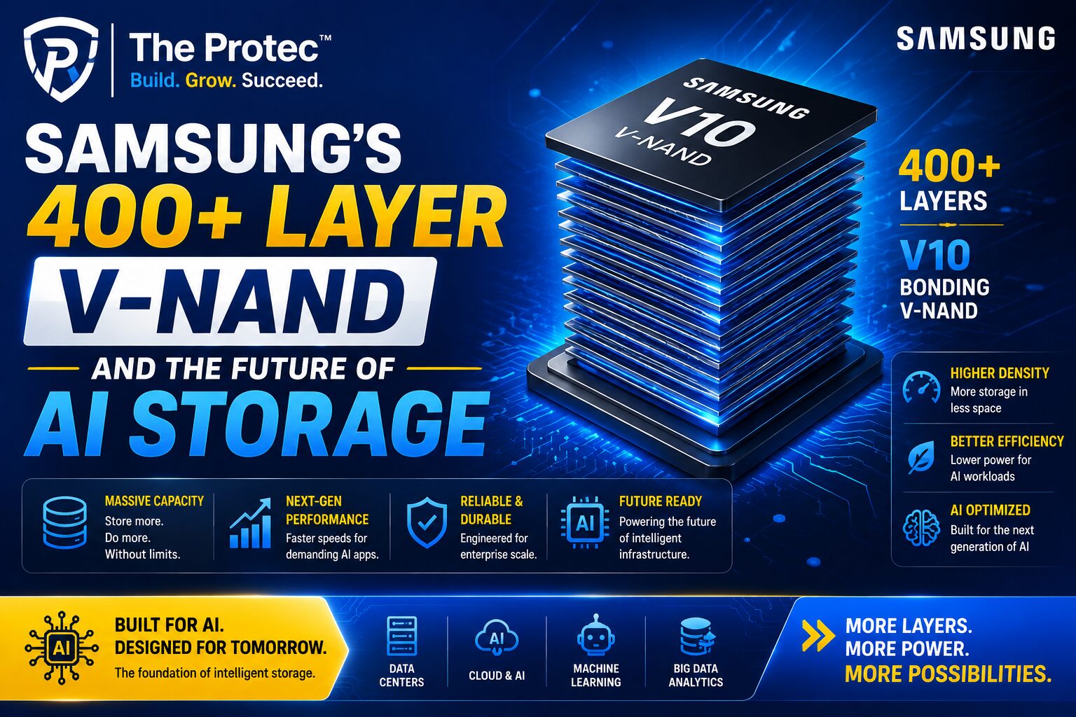
Samsung’s latest advances in flash memory are more than another jump in layer count. The company’s next-generation V10 Bonding V-NAND, often discussed as Samsung BV-NAND, represents a meaningful shift in how high-capacity storage can be built for the AI era. With 400+ layer NAND on the horizon, Samsung is targeting a problem that now sits at the center of modern computing: how to store, move, and serve massive volumes of data without overwhelming power, space, and cost budgets.
That matters because AI systems are no longer limited by compute alone. Large language models, recommendation engines, multimodal pipelines, vector databases, and real-time analytics all depend on storage infrastructure that can keep up with exploding data volumes. In that environment, Samsung V-NAND is not simply about adding more gigabytes per package. It is about improving storage density, reducing energy per bit, and enabling enterprise SSDs that can better support AI servers and data centers under relentless load.
For infrastructure teams, the practical question is simple: what does 400+ layer NAND actually change? The answer goes far beyond marketing numbers. It affects how much capacity can fit into a rack, how efficiently a storage array can operate, and how well AI workloads can sustain performance as datasets continue to grow. Samsung’s BV-NAND approach is designed to address these pressure points directly.
What Samsung BV-NAND Is and Why It Matters
BV-NAND stands for Bonding V-NAND, Samsung’s next step in 3D NAND architecture. Traditional 3D NAND already stacks memory cells vertically to increase capacity without expanding the die footprint. Bonding-based designs push that concept further by improving how memory structures are integrated, allowing more layers and better scaling potential than older fabrication approaches.
In simple terms, Samsung BV-NAND aims to do three things at once:
- Increase layer count dramatically, moving beyond 400 layers
- Improve density so more storage fits into the same physical space
- Reduce energy use per stored bit, which is critical for large-scale AI infrastructure
This is important because the storage industry has reached a point where raw capacity alone is not enough. Data centers now care deeply about watts per terabyte, thermal behavior, endurance, and latency consistency. A flash technology that adds capacity while also lowering operational overhead can influence procurement decisions across hyperscale, enterprise, and cloud environments.
Samsung has consistently been one of the most influential developers of V-NAND, and its latest direction reflects a broader industry trend: the move toward storage platforms that are optimized for AI-era workloads rather than generalized consumer use. For a deeper look at Samsung’s flash-memory portfolio, see Samsung’s official semiconductor resources at Samsung Semiconductor.
Why 400+ Layer NAND Is a Big Deal
Layer count has become one of the defining metrics in 3D NAND competition, but the number itself only tells part of the story. Crossing the 400-layer threshold is significant because it signals that the industry is pushing deeper into a new scaling regime. At this level, engineers are not just stacking more cells; they are also solving increasingly complex problems related to interconnects, signal integrity, cell uniformity, and manufacturing yield.
For Samsung V-NAND, the jump to 400+ layers can unlock several benefits:
- Higher storage density: More bits per wafer and more capacity per package mean smaller footprints for the same usable storage.
- Better cost efficiency over time: As density improves, the cost per terabyte can trend downward, especially in enterprise-scale deployments.
- Lower energy intensity: Packing more storage into fewer devices can reduce the power and cooling burden per terabyte.
- Improved scalability: Greater layer counts help manufacturers keep advancing capacity without relying solely on shrinking planar dimensions.
In a world where AI training and inference infrastructure is expanding rapidly, these gains are not academic. A large model training cluster may need vast amounts of fast storage for checkpointing, dataset staging, log retention, and retrieval-augmented generation pipelines. Every improvement in density and efficiency can translate into lower operating costs and better deployment flexibility.
How Samsung V10 Bonding V-NAND Fits Into AI Storage Technology
AI storage technology has changed dramatically in the last few years. Traditional storage systems were designed around transactional databases, file services, and general-purpose enterprise applications. AI workloads place different demands on storage: they require high-throughput data ingestion, rapid access to training corpora, efficient checkpoint writes, and stable performance under sustained pressure.
Samsung BV-NAND is relevant because it supports the kind of storage hierarchy AI systems increasingly need. Instead of relying solely on expensive, power-hungry compute nodes, infrastructure architects can use high-density flash to create faster staging layers and more efficient data pipelines. This is especially important for enterprises that are building private AI environments or hybrid cloud AI systems.
Here is where 400+ layer NAND can make a difference in AI storage technology:
- Dataset staging: Large training datasets can be kept closer to compute, reducing bottlenecks tied to slower storage tiers.
- Checkpointing: AI training jobs often write frequent snapshots; denser, more efficient SSDs can handle these writes with less overhead.
- Inference support: Retrieval systems, embeddings, and metadata stores benefit from high-capacity flash that can deliver predictable performance.
- Data lake acceleration: Flash-based caching and hot-tier storage help speed up analytics and model preparation workflows.
AI infrastructure is increasingly defined by how well it can move data, not just calculate on it. That is why Samsung V-NAND is strategically important: it helps make the storage layer an active enabler of AI performance rather than a passive bottleneck.
Storage Density: More Capacity in Less Space
One of the clearest advantages of Samsung’s 400+ layer V-NAND is storage density. Density matters because physical space in enterprise infrastructure is expensive. Every additional drive bay, rack unit, and server expansion comes with capital expense, operational cost, and cooling requirements.
By increasing the number of layers in a NAND stack, Samsung can store more data in the same silicon footprint. That creates a cascade of benefits for enterprise SSDs and data center operators:
- More terabytes per drive
- More usable capacity per server
- Fewer devices needed for the same workload
- Lower rack space requirements
- Potential reductions in cabling, power delivery, and maintenance overhead
For hyperscalers, density improvements can be especially valuable because the economics of scale amplify small gains. If an SSD generation can deliver more capacity without a corresponding rise in power draw or heat output, that can improve overall fleet efficiency. For enterprises, the value may be even more immediate: denser SSDs can simplify architecture and reduce the number of storage appliances required to support AI projects.
Samsung’s approach also reflects a broader market shift. As AI models become larger and data retention policies become more demanding, organizations want storage that scales vertically inside the same physical environment. 400+ layer NAND is one of the most direct ways to achieve that.
Energy Efficiency: The Hidden Advantage Behind BV-NAND
Capacity gets the headlines, but energy efficiency may be the more important story. Data centers are under pressure from rising power costs, thermal constraints, and sustainability goals. AI workloads intensify all three. Training and inference systems often run at high utilization, which means storage subsystems are no longer minor contributors to energy consumption.
Samsung BV-NAND is expected to help improve energy efficiency in several ways. First, higher density means fewer chips may be needed to reach a target capacity. Fewer components generally mean less aggregate power draw. Second, process and architectural improvements can reduce energy per operation, which matters for read-heavy and write-heavy enterprise environments. Third, better density can reduce the amount of cooling required per terabyte stored.
These gains may sound incremental, but at scale they are powerful. A data center operating tens of thousands of SSDs can see meaningful cost savings from even modest reductions in watts per drive. When multiplied across AI clusters, vector stores, and backup tiers, the operational impact becomes substantial.
Energy efficiency is also closely tied to sustainability reporting and procurement strategy. Organizations increasingly want infrastructure that supports growth without ballooning carbon footprint. Samsung V-NAND’s progression toward 400+ layers aligns with that requirement by making flash storage more efficient as capacity increases.
Why Enterprise SSDs Stand to Benefit First
While consumer storage products often attract attention, enterprise SSDs are where Samsung BV-NAND may matter most. Enterprise deployments demand endurance, predictable latency, and stable performance across mixed workloads. AI server environments place even more stress on those characteristics.
Enterprise SSDs built on 400+ layer NAND could offer:
- Higher capacity per drive for AI data repositories
- Improved power efficiency for dense server configurations
- Better cost per TB for large-scale storage purchases
- Support for hot and warm data tiers in AI pipelines
- Greater design flexibility for OEMs and cloud providers
For IT teams, this means storage strategy can become more aligned with workload patterns. Instead of treating flash as a premium tier reserved only for small hot datasets, organizations can deploy high-density SSDs more broadly across AI infrastructure. That can improve responsiveness and simplify data placement decisions.
It is also worth noting that the enterprise SSD market is evolving quickly. Buyers now evaluate not just sequential throughput, but also latency consistency, QoS under contention, and total cost of ownership. Samsung’s next-generation V-NAND is positioned to compete on all of those dimensions, especially as AI workloads grow more storage intensive.
How Samsung V-NAND Compares With the Broader NAND Roadmap
Samsung is not the only company pushing NAND scaling, but its BV-NAND roadmap stands out because of the emphasis on bonding and architectural evolution rather than simple incremental stacking. As layer counts rise across the industry, manufacturers must solve increasingly difficult engineering challenges. These include maintaining yield, preserving reliability, and avoiding performance degradation as cell structures become more complex.
That is why the move to 400+ layer NAND is more than a race for a bigger number. It is a test of manufacturing maturity and architectural design. Companies that can scale effectively will be better positioned to serve AI, cloud, and enterprise customers who need both capacity and efficiency.
For readers tracking the broader memory market, reports from industry analysts such as TrendForce often provide context on NAND supply, pricing, and technology transitions. See TrendForce for ongoing market coverage.
In practical terms, the companies that lead in next-generation NAND will likely shape how future data centers are built. Storage is becoming a strategic layer in AI architecture, and the vendor roadmap now matters almost as much as CPU or GPU selection.
What This Means for AI Servers and Data Centers
AI servers operate under a different set of constraints than traditional enterprise systems. They need to feed GPUs and accelerators with data quickly, avoid storage stalls, and support enormous datasets that grow over time. Data centers, meanwhile, must balance density, power, cooling, and operational resilience.
Samsung’s 400+ layer V-NAND can help on both fronts. In AI servers, higher-density flash can improve local storage configurations for model checkpoints, embeddings, feature stores, and preprocessing layers. In data centers, the same technology can reduce the physical and energy cost of storing increasingly large data volumes.
Some of the most important implications include:
- Better utilization of server space: More storage per drive helps reduce the number of devices installed per rack.
- Improved airflow and thermal management: Fewer drives or lower power per terabyte can simplify cooling design.
- More flexible AI deployment: Dense SSDs make it easier to build storage-rich inference and training nodes.
- Lower TCO for scale-out environments: Density and efficiency help reduce long-term infrastructure spending.
As AI systems mature, storage will increasingly be judged by how well it supports the entire data lifecycle. That includes ingestion, transformation, training, inference, archival, and retrieval. Samsung BV-NAND is designed to strengthen that foundation.
Challenges Samsung Still Needs to Solve
Even with the promise of 400+ layer V-NAND, there are still real engineering and market challenges. Higher layer counts can introduce manufacturing complexity, and the industry has to maintain reliability while continuing to improve cost and performance. Yield management, endurance, and consistency all become more difficult as designs become denser.
There is also the question of how quickly the ecosystem can adopt the new technology. Enterprise buyers typically move cautiously, especially in mission-critical deployments. They want proven reliability, strong firmware support, and compatibility with existing storage stacks.
That means Samsung’s BV-NAND success will depend not only on the memory itself, but also on how effectively it is integrated into enterprise SSD products and validated for real-world AI workloads. Still, the direction is clear: the market is demanding denser, more efficient flash, and Samsung is signaling that it intends to stay at the front of that shift.
Final Thoughts: Why Samsung BV-NAND Could Shape the Next Wave of AI Storage
Samsung’s 400+ layer V-NAND is more than a technology milestone. It is a response to a structural change in computing. AI has made storage a first-class infrastructure concern, and the next generation of flash has to do more than store data cheaply. It must help organizations scale faster, consume less power, and support increasingly complex workloads with predictable performance.
That is why Samsung BV-NAND is worth watching. By pushing Samsung V-NAND beyond 400 layers, the company is aiming to deliver the kind of capacity and efficiency gains that AI servers, data centers, and enterprise SSDs increasingly require. If the architecture performs as expected, it could influence everything from cloud deployment economics to on-prem AI infrastructure design.
For IT leaders, storage architects, and enterprise buyers, the message is straightforward: the next era of AI storage will be defined by density, efficiency, and scalability. Samsung’s latest NAND roadmap suggests that flash memory is still very much evolving to meet that challenge.
FAQ
What is Samsung BV-NAND?
Samsung BV-NAND, or Bonding V-NAND, is Samsung’s next-generation 3D NAND architecture designed to support much higher layer counts, improved density, and better energy efficiency for advanced storage products.
Why is 400+ layer NAND important for AI storage technology?
400+ layer NAND increases storage density and can reduce energy use per terabyte, which helps AI servers and data centers store more data in less space while improving overall efficiency.
How does Samsung V-NAND help enterprise SSDs?
Samsung V-NAND can enable higher-capacity SSDs with better power efficiency and potentially lower cost per terabyte, making it well suited for AI pipelines, cloud storage, and demanding enterprise workloads.
Will BV-NAND improve SSD performance as well as capacity?
The main benefits are density and efficiency, but architecture and firmware improvements can also support more consistent enterprise performance, especially under sustained workloads common in AI environments.
Is Samsung the only company working on next-generation NAND?
No. Other memory vendors are also advancing 3D NAND technologies, but Samsung’s bonding-based approach and 400+ layer roadmap make it one of the most closely watched developments in the market.