Contents
- 1 Why Chiplet Architecture Is the Future of CPUs and GPUs
- 2 What Chiplet Architecture Actually Means
- 3 Why Monolithic Chips Are Becoming Harder to Scale
- 4 How Chiplets Improve Yield and Lower Cost
- 5 Chiplet Architecture Unlocks Better Scalability
- 6 Performance Gains Come from Smarter Processor Design
- 7 Why Chiplets Are Ideal for Future CPUs
- 8 Why Chiplets Matter Even More for GPUs
- 9 The Role of Advanced Packaging and Interconnects
- 10 Chiplet Challenges That Still Need Solving
- 11 How Chiplets Are Changing the Economics of Processor Design
- 12 What This Means for the Next Generation of Processors
- 13 FAQ: Chiplet Architecture and the Future of CPUs and GPUs
- 14 Conclusion
Why Chiplet Architecture Is the Future of CPUs and GPUs
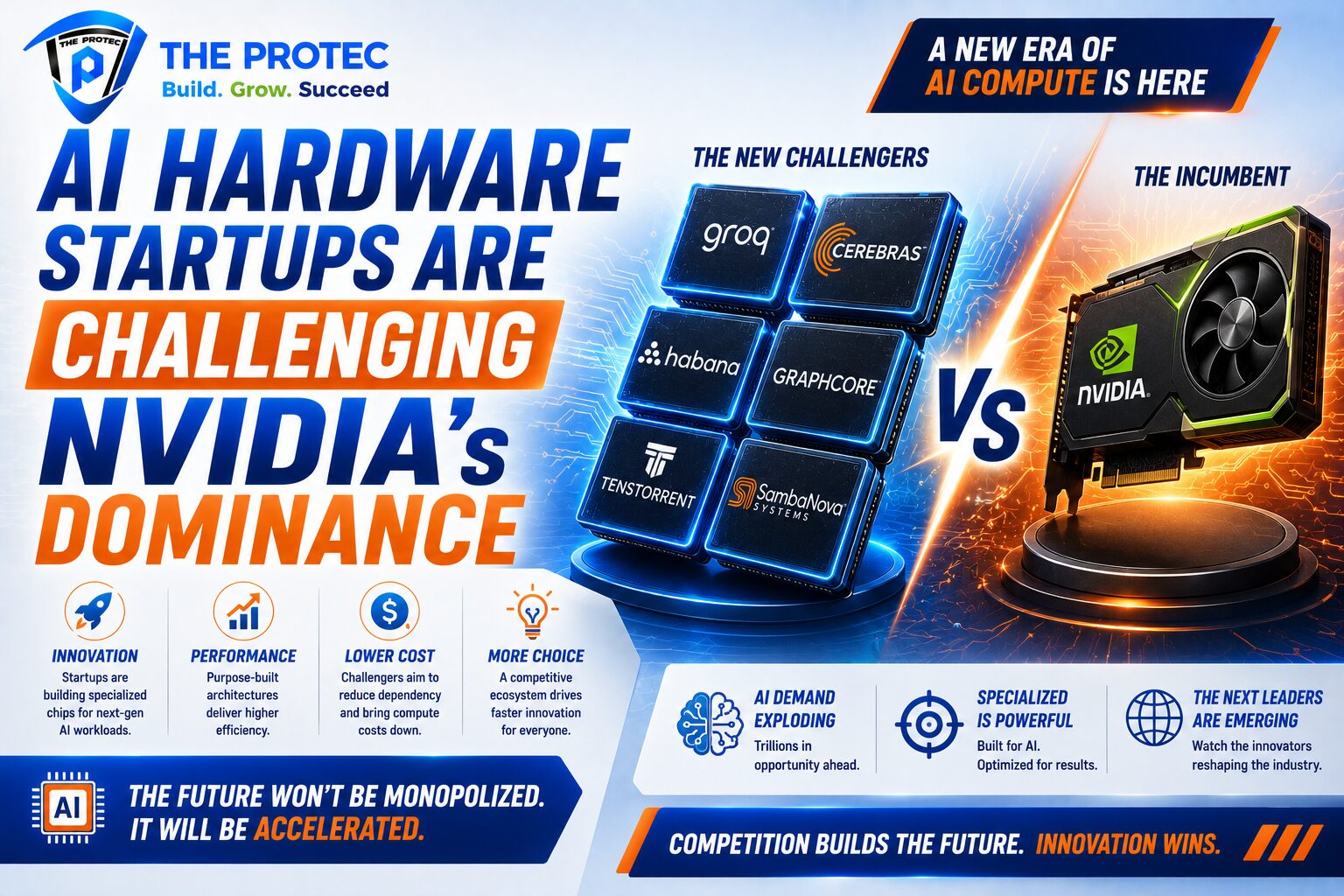
The processor industry is undergoing one of its biggest shifts in decades. For years, the dominant model in processor design was the monolithic chip: one large silicon die containing all major compute, cache, memory interface, and graphics logic. That approach worked well when transistor scaling was easier and performance gains could be achieved by simply shrinking nodes and increasing clock speeds. But as manufacturing has become more complex, expensive, and physically constrained, the old model has started to show its limits.
Enter chiplet architecture. Instead of building everything on a single enormous die, manufacturers now divide a processor into smaller specialized dies, or chiplets, and connect them with high-speed interconnects. This modular approach is rapidly becoming the preferred direction for future CPUs and GPUs because it improves yield, reduces cost, increases scalability, and gives designers more freedom to mix process nodes and optimize each part of the chip independently.
This is not a niche idea anymore. Chiplets are now central to the most advanced processor roadmaps in the industry, from server CPUs and desktop processors to high-end GPUs and AI accelerators. As workloads become more specialized and demand grows for more performance per watt, chiplet architecture is emerging as the new foundation of modern processor design.
What Chiplet Architecture Actually Means
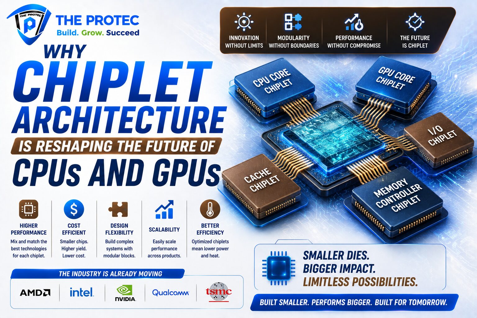
Chiplet architecture breaks a processor into smaller functional blocks rather than forcing every component onto one giant silicon die. These blocks can include CPU cores, cache, memory controllers, I/O logic, graphics engines, and accelerators. Each chiplet is manufactured separately and then assembled into a single package.
In practical terms, this means a company can design a processor like a system of modular parts instead of one monolithic piece of silicon. A compute chiplet may use the most advanced manufacturing process to maximize speed and efficiency, while an I/O chiplet may use a more mature node that is cheaper and more suitable for connectivity circuitry. The result is a more flexible processor platform.
The industry-standard concept here is often described as a “disaggregated” processor. The goal is not only to improve performance, but also to build processors that are easier to scale across product tiers. A vendor can reuse the same chiplet in multiple products, changing only the number of chiplets or the package configuration to target different markets.
Why Monolithic Chips Are Becoming Harder to Scale
Traditional monolithic designs are increasingly difficult to justify for the largest CPUs and GPUs. The basic problem is simple: the bigger the die, the harder it is to manufacture efficiently. Even a tiny defect can ruin a large chip, which lowers yield and increases cost. As dies become larger and more advanced, the economics get worse.
There are also physical and architectural limits. Larger dies face more challenges in power delivery, heat dissipation, and signal timing. At advanced process nodes, transistor density improves, but so do design complexity and costs. The gains from shrinking a single die are no longer as straightforward as they once were.
For GPUs, the problem is even more pronounced. Modern graphics chips and AI-oriented accelerators demand enormous compute density, large memory bandwidth, and sophisticated control logic. Building all of that on one die can become prohibitively expensive and risky. Chiplet architecture offers a cleaner path forward by allowing each function to be optimized separately.
How Chiplets Improve Yield and Lower Cost
One of the strongest reasons chiplet architecture is replacing monolithic chip designs is manufacturing yield. In semiconductor production, yield refers to the percentage of dies on a wafer that are functional. A very large die has a higher probability of containing a defect than a smaller die. By dividing a processor into multiple smaller chiplets, manufacturers reduce the risk that one flaw will destroy the entire product.
This has major economic benefits. Better yield means more usable dies per wafer, lower cost per chip, and less waste. It also makes it easier to build larger, more ambitious processors without carrying the full cost penalty of a giant monolithic design.
Chiplets also improve product binning and reuse. A vendor can test individual chiplets and combine them into different performance tiers, rather than discarding partially functional large dies. That flexibility is especially valuable in high-volume markets like data center CPUs, workstation processors, and premium GPUs.
Chiplet Architecture Unlocks Better Scalability
Scalability is one of the most compelling advantages of chiplet architecture. Instead of designing a completely new monolithic die for every performance tier, engineers can build a modular processor family from the same core components. This gives them far more control over core count, cache size, memory support, and power envelope.
For future CPUs, this is particularly important. A chiplet-based CPU can scale from a compact consumer processor to a massive server-class platform simply by varying the number of compute chiplets and the supporting die. That makes the product stack easier to maintain and faster to bring to market.
For GPUs, scalability is equally important. Graphics and compute workloads continue to grow in parallel, and AI-driven applications are putting pressure on memory bandwidth and parallel execution. Chiplets allow GPU designers to separate compute resources from other functions, which can make it easier to build larger and more specialized products.
The modular model also improves roadmap flexibility. If one chiplet design is strong, it can be reused across multiple generations or product lines with updates to the package, interconnect, or supporting dies. This reuse reduces development risk and shortens the time needed to launch new products.
Performance Gains Come from Smarter Processor Design
Chiplet architecture is not just about cost savings. It can also improve real-world performance. One advantage is that different parts of a processor can be built on the most appropriate process node. Performance-critical logic can use leading-edge silicon, while less demanding functions can use a mature node. That balance can improve both frequency and efficiency.
Another benefit is cache and memory placement. By separating compute chiplets from I/O and cache, designers can create more efficient data paths and reduce some of the trade-offs that come with monolithic layouts. In many modern processors, especially server CPUs, this structure allows better balancing of bandwidth and latency.
Chiplets also support more advanced heterogenous designs. Rather than forcing all cores to behave identically, processor teams can combine different types of compute blocks, accelerators, and memory structures. This is increasingly relevant for AI, machine learning, and graphics pipelines, where general-purpose cores alone are not enough.
It is important to note that chiplets are not automatically faster in every scenario. The interconnect between chiplets must be extremely fast and efficient, or the design can suffer from added latency. But as packaging and interconnect technologies improve, the performance trade-off is becoming much more favorable.
Why Chiplets Are Ideal for Future CPUs
CPU design has changed dramatically as single-thread performance gains have slowed and multi-core computing has become the norm. The future of CPUs depends on higher core counts, better power efficiency, and tighter integration with memory and I/O. Chiplet architecture fits that direction perfectly.
Modern CPU chiplets can be optimized for core density and cache, while a separate die handles memory controllers, PCIe lanes, and other connectivity functions. This separation allows CPU vendors to tune each part independently. It also supports faster innovation because an updated compute chiplet can be paired with an existing I/O die or vice versa.
That modularity matters even more in enterprise and cloud environments. Data center buyers want configurable systems that can be tailored to different workloads, whether that means virtualization, database processing, high-performance computing, or AI inference. Chiplet-based CPUs can deliver that flexibility without requiring a complete redesign for each market segment.
As the industry continues to prioritize performance per watt, chiplets give CPU architects a better way to balance power, thermals, and compute density. That is a key reason chiplet architecture is becoming the default answer to what future CPUs should look like.
Why Chiplets Matter Even More for GPUs
GPUs face a different set of pressures than CPUs. They must deliver huge amounts of parallel compute while also supporting massive memory bandwidth and increasingly complex workloads in gaming, rendering, simulation, and AI. Monolithic designs can still work, but they become difficult to scale efficiently as die sizes climb.
Chiplets help GPU designers solve this problem by separating the graphics core, memory interface, cache, and control logic into different dies. This approach can make it easier to build larger GPUs without the extreme yield penalties of one giant die. It also creates room for more aggressive specialization.
In the AI era, that specialization is especially valuable. GPUs are no longer just graphics engines; they are general-purpose compute platforms used for training and inference. Chiplets can help vendors optimize parts of the GPU for different roles, such as matrix math, rasterization, or memory-intensive tasks.
For consumers, that could eventually mean more powerful graphics cards with better efficiency and more predictable scaling across price points. For data centers, it could mean accelerators that are easier to expand into massive multi-die packages while controlling cost and thermal load.
The Role of Advanced Packaging and Interconnects
Chiplet architecture depends on advanced packaging. Without fast, efficient interconnects, chiplets would behave like loosely connected parts rather than a unified processor. The real breakthrough is not just splitting the silicon; it is enabling those separate dies to communicate with very low latency and high bandwidth.
Today, the industry is investing heavily in 2.5D and 3D packaging, through-silicon vias, interposer technology, and high-speed die-to-die links. These technologies reduce the physical distance between chiplets and improve signal integrity. The result is a package that behaves much more like a single integrated system.
Standards are also helping the ecosystem mature. The Universal Chiplet Interconnect Express (UCIe) initiative is one of the most important efforts to make chiplets more interoperable across vendors and platforms. For more on the standard itself, see the official UCIe site: https://www.uciexpress.org/.
Advanced packaging is now as strategically important as transistor scaling. In many cases, it determines whether chiplet design is practical at all. As packaging improves, chiplets become more competitive with traditional monolithic designs in both performance and cost.
Chiplet Challenges That Still Need Solving
Chiplet architecture is powerful, but it is not without challenges. One of the biggest is latency. When compute is spread across multiple dies, communication overhead can become a bottleneck if the interconnect is not carefully designed. This is why cache coherency, bandwidth, and physical layout are so critical.
Power delivery and thermal management are also more complex in multi-die packages. Engineers must ensure that each chiplet receives stable power and that heat is distributed effectively across the package. Packaging density can create new constraints that monolithic designs do not face in the same way.
There is also a design and validation challenge. A chiplet-based processor can be more difficult to test because the system behaves as an integrated package even though it is built from multiple dies. That increases the need for robust verification, software support, and platform tuning.
Despite these issues, the industry has been steadily solving them. The pace of progress in packaging, interconnect standards, and design tools suggests that chiplet-based systems will continue to improve rapidly over the next several product cycles.
How Chiplets Are Changing the Economics of Processor Design
Beyond the technical advantages, chiplets are changing the business model of processor development. Traditional monolithic design requires massive investment in one large die with a narrow range of reuse. That creates significant risk if the chip underperforms or manufacturing yields disappoint.
Chiplets reduce that risk by making processor development more modular. A company can invest in a high-value compute chiplet and then adapt it across several products. That not only improves return on engineering investment, but also speeds up portfolio expansion.
This economic shift is especially important as semiconductor development costs rise. Advanced nodes are expensive, and the timeline for bringing a new chip to market is long. Chiplets help spread those costs across more products and more markets, which is why they are so attractive for future CPUs and GPUs alike.
In effect, chiplets make processor design more like platform design. Instead of treating every new chip as a one-off project, manufacturers can build a reusable ecosystem of dies, packages, and interconnects.
What This Means for the Next Generation of Processors
The move toward chiplet architecture is not a temporary trend. It is a structural response to the limits of monolithic scaling and the growing demand for specialization. Future CPUs will likely rely on modular compute, flexible cache structures, and dedicated I/O chiplets. Future GPUs will continue moving toward multi-die designs that can scale compute more efficiently than one giant slab of silicon.
As packaging and interconnect technology continue to advance, chiplets will become even more attractive. We can expect tighter die-to-die integration, more heterogeneous combinations of compute and acceleration, and broader adoption across client, workstation, server, and AI markets.
For users, the benefits should show up as better performance per watt, more accessible high-end processors, and faster innovation cycles. For manufacturers, chiplets provide a practical way to keep pushing performance forward without relying on the old monolithic model.
The future of processor design is not about making one perfect chip. It is about composing the right chiplets into the right system. That is why chiplet architecture is becoming the default strategy for the next era of CPUs and GPUs.
FAQ: Chiplet Architecture and the Future of CPUs and GPUs
What is chiplet architecture in processor design?
Chiplet architecture is a design approach where a processor is split into multiple smaller dies, each handling specific functions such as compute, cache, memory, or I/O. These chiplets are assembled into one package and connected through high-speed interconnects.
Why are chiplets better than monolithic chips?
Chiplets improve manufacturing yield, reduce cost, increase scalability, and allow different parts of a processor to be built on the most suitable process node. They also make it easier to reuse designs across multiple product tiers.
Will chiplets replace monolithic processors completely?
Not entirely. Smaller and simpler chips will still use monolithic designs where they make sense. But for high-end CPUs, GPUs, and accelerators, chiplets are becoming the dominant architecture because they solve many of the scaling problems of large monolithic dies.
Do chiplets hurt performance because of interconnect latency?
They can if the design is poor, but modern packaging and die-to-die interconnects have reduced this concern significantly. The performance trade-off is often outweighed by the gains in yield, scalability, and flexibility.
Why are chiplets important for AI processors?
AI workloads need enormous compute density, memory bandwidth, and specialized acceleration. Chiplets make it easier to combine these capabilities in one package and scale them efficiently for training and inference.
Conclusion
Chiplet architecture is more than a clever packaging trick. It is a fundamental shift in processor design that addresses the real limitations of modern silicon manufacturing. By splitting CPUs and GPUs into modular dies, the industry can build faster, more efficient, more scalable, and more economically viable processors.
As the demand for compute continues to rise across gaming, cloud, enterprise, and AI workloads, chiplets will play a central role in shaping future CPUs and GPUs. The monolithic era is not disappearing overnight, but the direction is clear: the future belongs to flexible, modular, chiplet-based processor design.